Welcome to ExtremeHW
Welcome to ExtremeHW, register to take part in our community, don't worry this is a simple FREE process that requires minimal information for you to signup.
Registered users can:
- Start new topics and reply to others.
- Show off your PC using our Rig Creator feature.
- Subscribe to topics and forums to get updates.
- Get your own profile page to customize.
- Send personal messages to other members.
- Take advantage of site exclusive features.
- Upgrade to Premium to unlock additional sites features.

Sir Beregond
-
Posts
2,052 -
Joined
-
Last visited
-
Days Won
58 -
Feedback
100%
Content Type
Forums
Store
Events
Gallery
Profiles
Videos
Marketplace
Tutorials
Everything posted by Sir Beregond
-

guru3d Intel Battlemage GPUs December 3rd
Sir Beregond replied to UltraMega's topic in Hardware News
Wouldn't mind getting my hand on one to play with, but also interested in the higher end models. -
Haha, trust me, I totally get it. Its a weird time and I hope the same as you.
-
Lol. Chiplets for AMD started with EPYC server products, so not sure that is really the correct description. But I get the sentiment , and definitely monolithic is superior for latency purposes. And then there is Threadripper as well which is definitely not a gaming product. Intel besides first using chiplets for Meteor Lake also used them for Sapphire Rapids server chips.
-
That's good to hear. One of my biggest complaints with my 5900X is my RAM frequency is directly limited by my FCLK (fabric) frequency, since for Zen 3 and prior it had to be in a 1:1 ratio. My 5900X won't do any higher than 1866 FCLK so leaves me stuck at 3733 for the DDR4. Well, look forward to seeing how this progresses!
-
Huh that sounds like a bug for sure. Yeah I really don't like Ryzen Master myself either. Maybe just old school that way, but much prefer to manage all those settings in BIOS properly. Glad to hear you are enjoying it! Nice loop, love the functional nature of it. Looks like going to external rad? I thought it might be a good idea to try watercooling the RAM when I upgrade platforms to DDR5. How is the RAM working out on the 9950X?
-
Nice! Looks like you are having fun! With the fixed voltage (also what I do when OCing) and using a split CCD model of Ryzen, are you going about it with an all-core OC, or does your motherboard support per CCX all-core OCing? I found on my 5900X that the 1st CCD/CCX is descent enough binning (not great), but my 2nd CCD/CCX is pretty awful by comparison where the max all-core I can get out of the 2nd is at least 150MHz lower than the 1st. Being able to split my all-core settings between the two and pushing my better CCD to its brink is how I got my best score on R23 multi. Overall the bin I got as a package is kinda meh tier, but thought I might mention.
-
If I recall the RMx series (not to be confused with the cheaper RM series with no x) has the Japanese capacitors FWIW. Just going off that site, the Corsair warranty is 10 years while the MSI is 5 years. If these were my only two options, I'd go with the Corsair. Better warranty, and Japanese capacitors for the RMx model would make it just a better buy if these are the same price. But it would also be worth looking at options from Seasonic, Leadex / Superflower, beQuiet as well.
-
One correction: RTX 4080 had the $1199 MSRP. MSRP for the RTX 4080 Super was $999.
-
Ah, yeah did not mean that specifically for STALKER. Was more speaking in general how Microsoft has been buying up game studios over the past several years.
-
I don't like that Microsoft is buying up everyone. At the same time probably keeping the lights on for some places by doing so. Weird market.
-
Wow, either some serious pump out, or convexity.
-
"Second star to the right, and straight on till morning."
Sir Beregond replied to ENTERPRISE's topic in Announcements
I'd be curious the actual storage needs. What you lose with a single physical server in a house is dynamic scaling for increased activity / bursts of activity, redundancy for outages, etc. In my estimation of current site activity, probably not a big deal, but still things to consider. -
I don't think they've had just one flop. It's been a long time since anyone called Ubisoft "innovative" or really putting out something new. They've in many way phoned it in a lot.
-
Looking forward to seeing what you can do with it. Also lol to the last line!
-
I would agree with this. GPU of course is going to be the biggest boon at 4K. CPU might benefit 1% lows if you are on an old enough chip. Otherwise your averages are going to be pretty much the same at 4K.
-
How do you like the MSI board / BIOS so far? Been mostly on ASUS myself with some EVGA sprinkled in for the bench (Z490, Z790).
-
You....built an AMD system? Last thing I was expecting to read.
-
To be fair, I haven't ben playing many newer games lately.
-
Hadn't considered the DLSS factor. Good point. Maybe I will upgrade once 9800X3D hits $300ish.
-
Is that only on average FPS? @Slaughtahousemakes a good point, I should look at some of these reviews and see where the 1% lows have seen improvement. Otherwise, averages seem very flat at 4K, agreed.
-
"Second star to the right, and straight on till morning."
Sir Beregond replied to ENTERPRISE's topic in Announcements
Also wondering if the cost to develop the site is not reflected in the current activity of the site. Which is a shame, from a feature perspective, great site. -
Being on 4k, these 4k relative and actual performance charts put some things in perspective. I wonder how the 5090 will change these numbers come next year. AMD Ryzen 7 9800X3D Review - The Best Gaming Processor WWW.TECHPOWERUP.COM The Ryzen 7 9800X3D establishes AMD as the leader in gaming performance. This Zen 5-based X3D chip is not only fast, it also comes with full support for overclocking. Besides gaming, application...
-
Yeah I only mentioned Aquasuite if you had one of their fan controllers or something. Otherwise I think you'll be fine with the free software or this Argus.
-
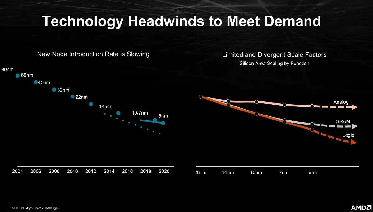
Yeah I think in many way yes, in some ways no. Analog components (your I/O, etc.) stopped scaling with new nodes way back in 28nm and maybe even before then. Cache was scaling well until around 7nm and has been leveling off since. Logic (your CPU / GPU cores, etc) on the other hand, continues to scale with each new process shrink, and actually looks like it might start scaling even better as we continue. Seems to suggest scaling is favoring logic these days while cache and analog transistors are already so much smaller than logic transistors, that they are probably already at their physical limits and in that sense, yeah Moore's Law is dead. And then yeah you mention the efficiency part which is interesting because on one hand companies are really trying to market themselves as efficient. Meanwhile the actual base power draw is so much more these days that they used to be. Top end GPUs used to max out at 250W. Now you have a 450W (default) 4090 that is arguably one of the most efficient power to performance GPUs Nvidia has released to the consumer market, yet its still drawing far more than we used to. Anyway, I'm interested in hardware still to an extent, but likewise hard to get excited about stuff when large market segments have stagnated and only gotten more expensive. Based on this chart from AMD, one of the reasons chiplets made sense. Logic on the most advanced node they want to use, meanwhile offload I/O component to older nodes because there is no reason to use the more advanced/expensive ones.

-
Good call out, and agreed.